Outer and inner layer tolerance limits
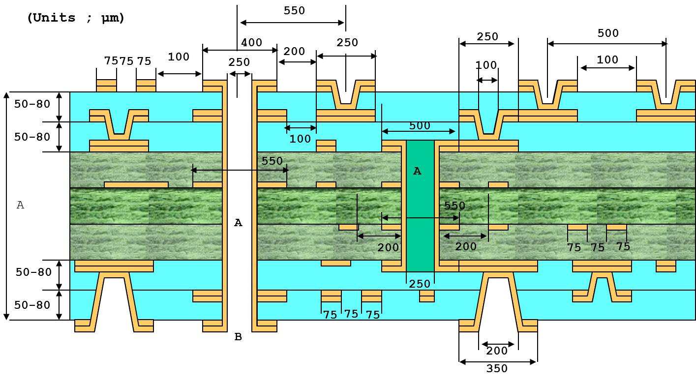
Design Rules Check for Inner layers can be ambiguous!
For inner layers a design rules check called “clearance trace to plated hole edge” is not always interpreted in the same way. See the above illustration immediately left of lower part of via hole A in green color. The double arrow marks the correct clearance distance to 200 (um). It must not be measured from the inner edge of the hole, which would be the result if plated (finished) hole size is used.
CAD systems however usually work with finished hole sizes which means that with 150 um (6 mil) over-size drill to allow for plating, 3 mil each side, a setting for this parameter of 200 um will leave 125 um to pass which is not safe to manufacture. The setting must be increased with the 75 um difference which brings it to 275 um, unless CAD system setting allows for this which is unusual. Serious amounts of rework or unusable layouts can result if this is not checked and corrected before a new CAD system is used.
Detailed Capability Information
Pad Size for Laser Drilling10 mil (Drill depth <65um), 11 mil (Drill depth <100um)6 mil8mil± 0.05mm1.5 mil
| Shipco Circuits Ltd. | PCB Manufacture Capabilities 2012 | ||||||||||||||||||||||
| Material Type | RCC Material | Copper thickness 12um, Resin thickness 65 and 100um | |||||||||||||||||||||
| LDPP (Laser Drill Prepreg Material) | IT-180A 1037(2.0 mil), IT-180A 1086 (3.0 mil) | ||||||||||||||||||||||
| FR4 Tg minimum 130 | S1144 – standard for 2 layer | FR4 Tg minimum 145 | S1141 150 – minimum Tg for lead free multilayer | Halogen Free Material FR4 Tg minimum 130 | S1155 | Halogen Free Material FR4 Tg minimum 170 | S1165 – for SMT prototypes if repeat soldering of components expected High Tg provides excellent pad bond strength | High Tg Material FR4 | FR408, IT180A, PLC-370HR, N4000-13, N4000-13SI | Hydrocarbon Ceramic High Frequency Material | Rogers 4350, Rogers 4003, Arlon 25FR, Arlon 25N | PTFE High Frequency Material | Rogers Series, Taconics Series, Arlon Series, Nelco Series | PTFE Bonding Film | RO3001 (1,5mil), HTI.5 (1,5mil), Cuclad 6700 (1,5mil) | ||||||||
| PTFE Prepreg Model | Gore Speed Board C ( 1.5, 2.0, 2.2, 3.4mil) Taconic TPG-30, 32, 35 ( 4.5, 5.0mil ) | ||||||||||||||||||||||
| Production Type | Rigid Board | Backplane, HDI, Blind & Buried via, Buried Capacitance, Buried Resistance, Electrical source thick copper, Back Drilling | |||||||||||||||||||||
| Lamination Model | Blind&Buried via Type | Mechanical Blind&Buried via with less than 3 times laminating | |||||||||||||||||||||
| HDI Type ( RCC and LDPP ) | 1+n+1, 1+1+n+1+1, 2+n+2(Buried via<0.3mm; only for RCC) The Laser Via can be filled with resin or copper | ||||||||||||||||||||||
| Surface Finish | Lead Free finishes: | HASL lead free, Flash Gold (Base copper <1oz, ENIG, Immersion Silver, Immersion Tin, OSP, Hard Gold Plating | |||||||||||||||||||||
| ENIG+OSP, ENIG+G/F, Flash Gold+G/F, Immersion Silver+G/F, Immersion Tin+G/F, ENEPIG | |||||||||||||||||||||||
| Lead finish only: | HASL (also now called Tin/Lead HASL) | ||||||||||||||||||||||
| Surface Plating or coating | solder thickness (HASL) | 2-40um ( minimum 0,4um on large area for HASL!) | |||||||||||||||||||||
| thicknesses | Flash Gold | Ni:2.5-5um, Au>0.025um | |||||||||||||||||||||
| ENIG | Ni:2.5-5um, Au 0.05-0.1um | ||||||||||||||||||||||
| Immersion Tin | Tin >= 1.0um | ||||||||||||||||||||||
| Immersion Silver | Silver: 0.1-0.3um | ||||||||||||||||||||||
| OSP | 0.2-0.3um | ||||||||||||||||||||||
| Hard Gold Plating | Au max 2.5um | ||||||||||||||||||||||
| ENEPIG | For soldering: Ni:3-5um Pd:0.05-0.1um Au:0.03-0.05um | ||||||||||||||||||||||
| For gold wire bonding: Ni:3-5um Pd:0.1-0.15um Au:0.07-0.15um | |||||||||||||||||||||||
| Carbon Thickness | 0.10-0.35mm | ||||||||||||||||||||||
| Solder Mask Thickness | 10-18um ( On copper area) 5-8um ( On via pad and line corner) | ||||||||||||||||||||||
| Peelable Solder Mask Thickness | 0.20-0.50mm | ||||||||||||||||||||||
| Hole | Hole Size(finished) Mechanical Drilling | 0.10-6.5mm | |||||||||||||||||||||
| A Min. Hole size is 0.25mm for PTFE Material | |||||||||||||||||||||||
| B The hole size is less than 0.30mm for blind & buried via | |||||||||||||||||||||||
| C The hole size is less than 0.30mm for plugging hole with solder mask in pad | |||||||||||||||||||||||
| D Min. Connection Hole size 0.35mm | |||||||||||||||||||||||
| E The hole size range is 0.10-0.40mm for plugging with resin | |||||||||||||||||||||||
| Hole Size(finished) Laser Drilling | A The blind hole size range is 0.075-0.15mm for plugging with resin | ||||||||||||||||||||||
| A The blind hole size range is 0.075-0.127mm for filling plating | |||||||||||||||||||||||
| Aspect Ratio | Max PCB THK 1.2mm for mecanical drilling tool diameter 0.15mm | ||||||||||||||||||||||
| Max PCB THK 0.6mm for mecanical drilling tool diameter 0.10mm | |||||||||||||||||||||||
| <16:1 (Tooling size >0.2mm) | |||||||||||||||||||||||
| Hole Position Tolerance | ± 3 mil | PTH Size Tolerance | ± 3 mil | Press PTH Size Tolernace | ± 2 mil | NPTH Size Tolerance | ± 2 mil ( Limited tolerance +0/-2 mil or +2/-0 mil ) | ||||||||||||||||
| The realation between hole size(finished) | 0.1mm & 0.15mm (board THK<1.6mm), 0.2mm (board THK<2.4mm ) | ||||||||||||||||||||||
| for plugging with resin and board thickness | 0.25mm (board THK<2.8mm ), 0.3mm (board THK<3.2mm ) | ||||||||||||||||||||||
| Min Laser Drill Hole Size | 0.10mm (Laser drill depth <65um), 0.13mm (Laser drill depth <100um) | ||||||||||||||||||||||
| The Range of Backdrill Hole Size | 0.5-6.5mm | ||||||||||||||||||||||
| The Space of Between the Target Layer | <0.20mm | ||||||||||||||||||||||
| Tolerance of Backdrill Dept | ±0.10mm | ||||||||||||||||||||||
| Countersink Size and Angle | Special drill bit: angle 82º, 90º, 120º (Hole size 0.3-10mm) | ||||||||||||||||||||||
| Normal drill bit: angle 130º (3.175mm), 165º (3.175-6.5mm) | |||||||||||||||||||||||
| Countersink Angle Tolerance | ±0.10º | Countersink Hole Size Tolerance | ±0.20mm | Countersink Depth Tolerance | ±0.15mm | Slot Size Tolerance for Routing | ±0.15mm | Depth Tolerance for Blind NPTH Slot Routing | ±0.10mm | Pad size | Min. | ||||||||||||
| Min. Pad Size for Mecanical Drilling | 14 mil (via 8 mil, Base copper 0.5oz and 1.0oz), 20 mil (via 8 mil, Base copper 2oz), 24 mil (via 8 mil, Base copper 3oz) | ||||||||||||||||||||||
| Min Pad Size for BGA | 7 mil | ||||||||||||||||||||||
| Pad Size Tolerance | +5% -10% | ||||||||||||||||||||||
| Line Width | Inner Layer | 1/3-1/2oz: 3/3 mil | |||||||||||||||||||||
| Line Space | 1oz: 3/4 mil | ||||||||||||||||||||||
| Capability | 2oz: 5/5 mil | ||||||||||||||||||||||
| 3oz: 6/7 mil | |||||||||||||||||||||||
| 4oz: 7/11 mil | |||||||||||||||||||||||
| 5oz: 10/16 mil | |||||||||||||||||||||||
| Outer Layer | Base copper 1/3oz(12um): 3/3 mil | ||||||||||||||||||||||
| Base copper 0.5oz / 3.5/3.5 mil | |||||||||||||||||||||||
| Base copper 1oz / 4.5/5 mil | |||||||||||||||||||||||
| Base copper 2oz / 6/8 mil | |||||||||||||||||||||||
| Base copper 3oz / 8/14 mil | |||||||||||||||||||||||
| Base copper 4oz / 10/16 mil | |||||||||||||||||||||||
| Base copper 5oz / 12/20 mil | |||||||||||||||||||||||
| Line With Tolerance | <10 mil: ±1.0 mil | ||||||||||||||||||||||
| >10 mil: ±1.5 mil | |||||||||||||||||||||||
| Space | Min gap between hole wall to line | ||||||||||||||||||||||
| (Blind and buried via PCB) | 9 mil ( 2 or 3 times lamination) | ||||||||||||||||||||||
| Min gap between hole wall to line | |||||||||||||||||||||||
| (None blind and buried via PCB | 6 mil (<8 layre), 8 mil (<14 layer), 9 mil (<28 layer) | ||||||||||||||||||||||
| Min gap between laser to line (HDI PCB) | |||||||||||||||||||||||
| Min gap between outline and pattern | |||||||||||||||||||||||
| for no copper exposure after routing | 8 mil | ||||||||||||||||||||||
| V-CUT no copper exposure, distance | |||||||||||||||||||||||
| between V-cut line and Circuit (mm) | H<1.0mm: 0.3 (20º ), 0.33 (30º ), 0.37 (45º ), 0.42 (60º ) | ||||||||||||||||||||||
| 1.0 <H<1.6mm: 0.36 (20º ), 0.4 (30º ), 0.5 (45º ), 0.6 (60º ) | |||||||||||||||||||||||
| 1.6 <H<2.4mm: 0.42 (20º ), 0.51 (30º ), 0.64 (45º ), 0.8 (60º ) | |||||||||||||||||||||||
| 2.5 <H<3.0mm: 0.47 (20º ), 0.59 (30º ), 0.77 (45º ), 0.97 (60º ) | |||||||||||||||||||||||
| Min width for the Isolation Tape Innerlayer | 8mil | ||||||||||||||||||||||
| Min gap between hole wall (Same Net) | |||||||||||||||||||||||
| Min gap between pads for Immersion Gold | 4 mil | ||||||||||||||||||||||
| Min gap between Gold fingers | 6 mil | ||||||||||||||||||||||
| Min gap between pads for HASL | 7 mil (10 mil on large copper area) | ||||||||||||||||||||||
| Min gap between Peelable soldermask and pad | 16 mil | Min gap between Legend and Pad | 6 mil | Min gap between Carbone Pads | 15 mil | Metal Base | No of Metal base PCB Layer | 2-4 layer | PCB | Outline Machining dimension tolerance | (including blind slot depth) | ||||||||||||
| Surface finish of PCB | HASL, Flash Gold (Base copper<1oz), ENIG, Immersion Silver, Immersion Tin, OSP, Hard gold plating, ENEPIG | ||||||||||||||||||||||
| Surface finish of Metal Base | Cu: Ni&Au Plating, Al: Anodic oxidation, Hard anodic oxidation coating, Chemical passivation | ||||||||||||||||||||||
| Thermal Conductivity | 1- 4 W/mK | ||||||||||||||||||||||
| Metal Base PCB | Prebonding, Postbonding, Agglomerate Metal PCB technics, Metal core PCB, Buried Metal | ||||||||||||||||||||||
| Others | Min Core thickness | 0.05mm (No blind and buried via PCB), 0.13mm (blind and buried via PCB) | |||||||||||||||||||||
| No. Of PCB Layers | 2 – 40 | ||||||||||||||||||||||
| PCB thickness | 0.13 – 7.0mm (If the boards THK<0.5mm, the panel size must be<18 inch) | ||||||||||||||||||||||
| Max. Board size | 23 x 35 inch | ||||||||||||||||||||||
| Register tolerance between layers | <5 mil | ||||||||||||||||||||||
| PCB thickness tolerance | Thickness<1.0mm: ±0.1mm | ||||||||||||||||||||||
| Thickness>1.0mm: ±0.10% | |||||||||||||||||||||||
| Special PCB THK tolerance (Not include special layer by layer space demand) | |||||||||||||||||||||||
| Thickness<2.0mm: ±0.1mm, Thickness 2.1 – 3.0mm: ±0.15mm | |||||||||||||||||||||||
| Imedance tolerance | ± 5Ω (<50Ω), ±10% (>50Ω), >50Ω can be ± 5% | ||||||||||||||||||||||
| Outline dimension tolerance | ± 0.1mm | ||||||||||||||||||||||
| Outline location tolerance | ± 0.1mm | ||||||||||||||||||||||
| Min. varpage | 0.10 % | ||||||||||||||||||||||
| Max.finished copper on inner layer | 10oz | ||||||||||||||||||||||
| Min. isolation thickness between layer | 2 mil (only for base copper 0.5oz) | ||||||||||||||||||||||
| Min. Legend width and gap | Legend width: 4 mil, Legend high: 23 mil (for 12um and 18 um base copper) | ||||||||||||||||||||||
| Min. Internal radius | 0.3mm | ||||||||||||||||||||||
| V-CUT angle tolerance | ± 5º | ||||||||||||||||||||||
| V-CUT symmetrical tolerance | ± 4 mil | ||||||||||||||||||||||
| V-CUT rest thickness tolerance | ± 4 mil | ||||||||||||||||||||||
| Outline Machining | Routing: V-CUT, Tab connecting, Stamp holes | ||||||||||||||||||||||
| Min. Solder mask bridge width | 4 mil (for green), 5 mil (for other colors), If base copper <1oz can be 5 mil, If base copper 2 – 4oz can be 6 mil. | ||||||||||||||||||||||
| Min width of Solder mask cover line(Single side) | |||||||||||||||||||||||
| Solder mask color | Green, Yellow, Black, Blue, Red, White, Matte Green | ||||||||||||||||||||||
| Legend color | White, Yellow, Black | ||||||||||||||||||||||
| Angle tolerance of Gold finger | ±5º | ||||||||||||||||||||||
| Rest thickness tolerance of Gold finger chamfer | ±5 mil | ||||||||||||||||||||||
| Max Test voltage | 500V | ||||||||||||||||||||||
| Max Test currency | 200mA | ||||||||||||||||||||||
| Legend print mark type(only for white color) | Serial number, Bar code, Planar code |